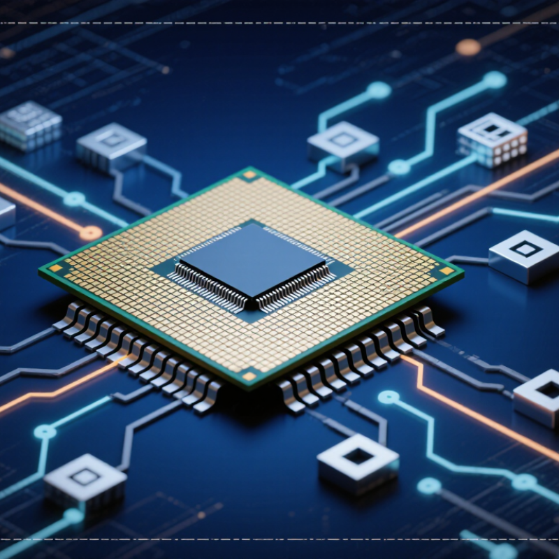
An FPGA integrated circuit contains configurable logic blocks, routing resources, memory elements, and input/output interfaces. Engineers describe intended behavior with HDL, often at register-transfer level, before hardware resources are assigned. A clocked counter, packet filter, or control state machine becomes synthesizable logic. The result is not software running on a processor. It is a programmed electrical structure.
During synthesis, tools parse HDL, infer registers, simplify Boolean expressions, and map functions into available primitives. Poorly written loops or incomplete assignments can create unintended storage or excessive logic. I have found that readable RTL usually makes timing problems easier to trace, although readability alone cannot guarantee efficiency. Constraints then define clock periods, input delays, output delays, and relationships between clock domains. Missing constraints are dangerous.
Placement assigns each logical element a physical location on the chip. Routing connects those locations through programmable wires and switches, while timing analysis measures delay across every critical path. If a data path misses its deadline, engineers may pipeline it, reduce fanout, restructure arithmetic, or adjust placement guidance. Timing closure is iterative, not ceremonial. A design can pass synthesis and still fail after routing because wire delay dominates a crowded region. Reviewing reports, checking clock-domain crossings, and testing reset behavior provide evidence beyond a clean compilation. One practical weakness remains: estimates change as the design grows. Measure early.